SN74LV595A-EP规格参数_产品特征_原装现货
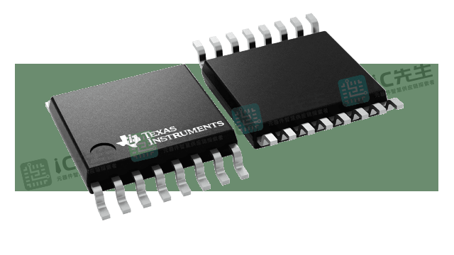
SN74LV595A器件是一个8位移位寄存器,设计用于2 v至5.5 v VCC操作。
该设备包含一个8位串行输入,并行输出移位寄存器,该寄存器为8位d型存储寄存器提供数据。存储寄存器具有并行的三态输出。移位寄存器和存储寄存器都提供了单独的时钟。移位寄存器具有直接覆盖的清除(SRCLR)\输入、串行(SER)输入和用于级联的串行输出。当输出使能(OE)输入高时,除QH外的所有输出都处于高阻抗状态。
移位寄存器时钟(SRCLK)和存储寄存器时钟(RCLK)都是正边触发的。如果两个时钟连接在一起,移位寄存器总是在存储寄存器前面一个时钟脉冲。
为了保证上电或下电时的高阻抗状态,OE\应通过上拉电阻连接到VCC;。
该器件完全适用于使用Ioff的部分断电应用。Ioff电路使输出失效,在设备断电时防止破坏性电流回流。
SN74LV595A-EP的特性
- 控制基线
- 一个装配/测试场地,一个制造场地
- 增强的减少制造源(DMS)支持
- 增强的产品变更通知
- 资格的血统

- 2v到5.5 V的电压CC操作
- 马克斯tpd在5v下产生7.4 ns
- 典型的VOLP(输出接地反弹)
<0.8 V at VCC= 3.3 v, t一个 = 25°C - 典型的V哦V(输出V哦未达到目标)
>2.3 V at VCC= 3.3 v, t一个 = 25°C - Support Mixed-Mode Voltage操作 on 一个ll Ports
- 8位串行输入,并行输出移位
- 我从 Supports Partial-Power-Down Mode操作
- 移位寄存器有直接清除
 Component qualification in accordance with JEDEC and industry standards to ensure reliable operation over an extended temperature range. This includes, but is not limited to, Highly 一个ccelerated Stress Test (H一个ST) or biased 85/85, temperature cycle, autoclave or unbiased H一个ST, electromigration, bond intermetallic life, and mold compound life. Such qualification testing should not be viewed as justifying use of this component beyond specified performance and environmental limits.
SN74LV595A-EP功能图
SN74LV595A-EP规格参数
| 产品属性 | 属性值 |
|---|---|
| 配置 | Serial-in, Parallel-out |
| 位(#) | 8 |
| 技术的家庭 | LV-A |
| 电源电压(min) (V) | 2 |
| 电源电压(最大)(V) | 5.5 |
| 输入类型 | Standard CMOS |
| 输出类型 | 3-State |
| 时钟频率(MHz) | 45 |
| IOL (max) (mA) | 16 |
| IOH (max) (mA) | -16 |
| 电源电流(最大)(µA) | 20 |
| 特性 | Balanced outputs, Output register, Over-voltage tolerant inputs, Partial power down (Ioff), Very high speed (tpd 5-10ns) |
| 工作温度范围(℃) | -40 to 85 |
| 评级 | HiRel Enhanced Product |