新闻详情
客服


SN74LVC74A-EP规格参数_产品功能_原装原厂
322 2023-12-01 09:58:34 来源: 网络 作者: IC先生
SN74LVC74A双正极触发d型触发器设计用于2.7 v至3.6 v的VCC工作。
预设(PRE)或清除(CLR)输入端的低电平设置或重置输出,而不考虑其他输入的电平。当PRE和CLR处于非活动状态(高)时,满足设置时间要求的数据(D)输入端的数据被传输到时钟脉冲正沿的输出端。时钟触发发生在电压水平上,与时钟脉冲的上升时间没有直接关系。在保持时间间隔之后,可以改变D输入端的数据,而不影响输出端的电平。
输入可以从3.3 V或5 V设备驱动。该特性允许在混合3.3 V/5 V系统环境中使用该设备作为转换器。
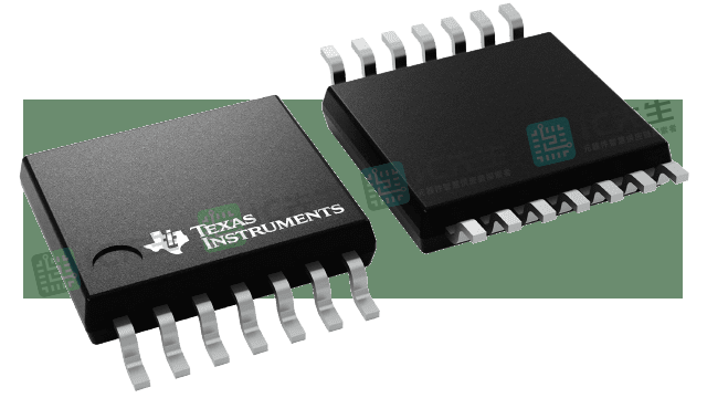
SN74LVC74A-EP的特性
- 控制基线
- 一个装配/测试场地,一个制造场地
- Extended Temperature Performance of -40°C to 125°C and -55°C to 125°C
- 增强的减少制造源(DMS)支持
- 增强的产品变更通知
- 资格的血统(1)
- 操作从2v到3.6 V
- 输入接收电压为5.5 V
- 马克斯tpd在3.3 V下产生5.2 ns的电流
- 典型的VOLP (Output Ground Bounce) <0.8 V at VCC= 3.3 v, t一个 = 25°C
- 典型的V哦V(输出V哦 Undershoot) >2 V at VCC= 3.3 v, t一个 = 25°C
(1)Component qualification in accordance with JEDEC and industry standards to ensure reliable operation over an extended temperature range. This includes, but is not limited to, Highly 一个ccelerated Stress Test (H一个ST) or biased 85/85, temperature cycle, autoclave or unbiased H一个ST, electromigration, bond intermetallic life, and mold compound life. Such qualification testing should not be viewed as justifying use of this component beyond specified performance and environmental limits.
SN74LVC74A-EP功能图
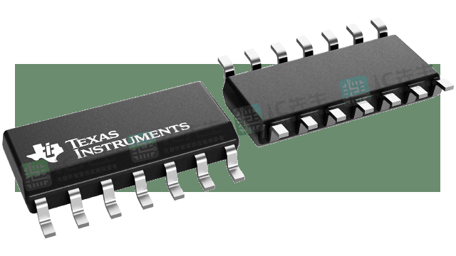
SN74LVC74A-EP规格参数
| 产品属性 | 属性值 |
|---|---|
| 通道数 | 2 |
| 技术的家庭 | LVC |
| 电源电压(min) (V) | 2 |
| 电源电压(最大)(V) | 3.6 |
| 输入类型 | Standard CMOS |
| 输出类型 | Push-Pull |
| 时钟频率(max) (MHz) | 100 |
| IOL (max) (mA) | 24 |
| IOH (max) (mA) | -24 |
| 电源电流(最大)(µA) | 10 |
| 特性 | Balanced outputs, Over-voltage tolerant inputs, Very high speed (tpd 5-10ns) |
| 工作温度范围(℃) | -40 to 125, -55 to 125 |
| 评级 | HiRel Enhanced Product |
版权声明:
部分文章信息来源于网络以及网友投稿,本网站只负责对文章进行整理、排版、编辑,是出于传递更多信息之目的,并不意味着赞同其观点或证实其内容的真实性,如本站文章和转稿涉及版权等问题,请作者及时联系本站,我们会尽快处理。
文章标签:
芯片
841次 2024-01-24 16:19:41
2534次 2024-01-03 17:20:40
1671次 2024-01-02 17:04:26
1230次 2023-12-28 17:30:12