SN74LVC540A-EP产品参数_产品功能_原装销售
SN74LVC540A-EP八进制缓冲器/驱动器设计用于2.7 v至3.6 v的VCC操作。
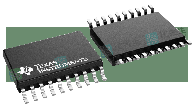
这个设备是理想的驱动总线线路或缓冲存储器地址寄存器。该器件的特点是输入和输出在封装的两侧,方便印刷电路板布局。
三态控制门是一个双输入与门,具有有效的低输入,因此,如果输出使能(OE1或OE2)输入高,则所有输出都处于高阻抗状态。
输入可以从3.3 v或5 v设备驱动。此功能允许在混合3.3 v /5 v系统环境中使用该设备作为转换器。
该设备完全指定为使用Ioff的部分断电应用程序。Ioff电路使输出失效,在设备断电时防止破坏性电流回流。
为确保上电或下电时的高阻抗状态,OE应通过上拉电阻与VCC连接;。
SN74LVC540A-EP的特性
- 控制基线
- 一个装配/测试场地,一个制造场地
- Extended Temperature Performance of –40°C to 125°C
- 增强的减少制造源(DMS)支持
- 增强的产品变更通知
- 资格的血统

- 操作从2v到3.6 V
- 输入接收电压为5.5 V
- 马克斯tpd在3.3 V下产生5.3 ns的电流
- 典型的VOLP (Output Ground Bounce) <0.8 V at VCC= 3.3 v, t一个 = 25°C
- 典型的V哦V(输出V哦 Undershoot) >2 V at VCC= 3.3 v, t一个 = 25°C
- Supports Mixed-Mode Signal Operation on 一个ll Ports (5-V 我nput/Output Voltage With 3.3-V VCC)
- 我从支持部分下电模式操作
 Component qualification in accordance with JEDEC and industry standards to ensure reliable operation over an extended temperature range. This includes, but is not limited to, Highly 一个ccelerated Stress Test (H一个ST) or biased 85/85, temperature cycle, autoclave or unbiased H一个ST, electromigration, bond intermetallic life, and mold compound life. Such qualification testing should not be viewed as justifying use of this component beyond specified performance and environmental limits.
SN74LVC540A-EP功能图

SN74LVC540A-EP规格参数
| 产品属性 | 属性值 |
|---|---|
| 技术的家庭 | LVC |
| 电源电压(min) (V) | 2 |
| 电源电压(最大)(V) | 3.6 |
| 通道数 | 8 |
| IOL (max) (mA) | 24 |
| IOH (max) (mA) | -24 |
| 电源电流(最大)(µA) | 10 |
| 输入类型 | Standard CMOS |
| 输出类型 | 3-State |
| 特性 | Balanced outputs, Very high speed (tpd 5-10ns) |
| 评级 | HiRel Enhanced Product |
| 工作温度范围(℃) | -40 to 125 |